Paradoxical Insight: The AI ecosystem perceived as less “frontier” (Google/Gemini) is building a more defensible economic moat than the model leader (Nvidia/OpenAI), because its core advantage isn’t in software, but in a structural hardware breakthrough: TPUs and the Optical Circuit Switch (OCS). This turns the exponential AI compute cost problem into a scalable profit engine.
OCS: The “Stupid” Network That Outsmarts Everyone
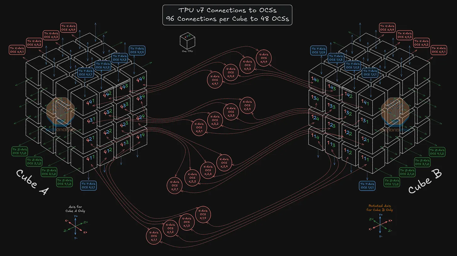
An OCS isn’t an optical transistor or a smart router. It’s a massive, reconfigurable patch panel for light. Using MEMS (micro-electromechanical systems) mirrors, it creates direct, dedicated fiber-optic highways between TPU chips on demand. OCS are essentially electrically-controlled microscopic mirrors (100 microns to 1 mm, about thickness of a human hair to the size of a grain of sand) that direct light data signals between TPUs.
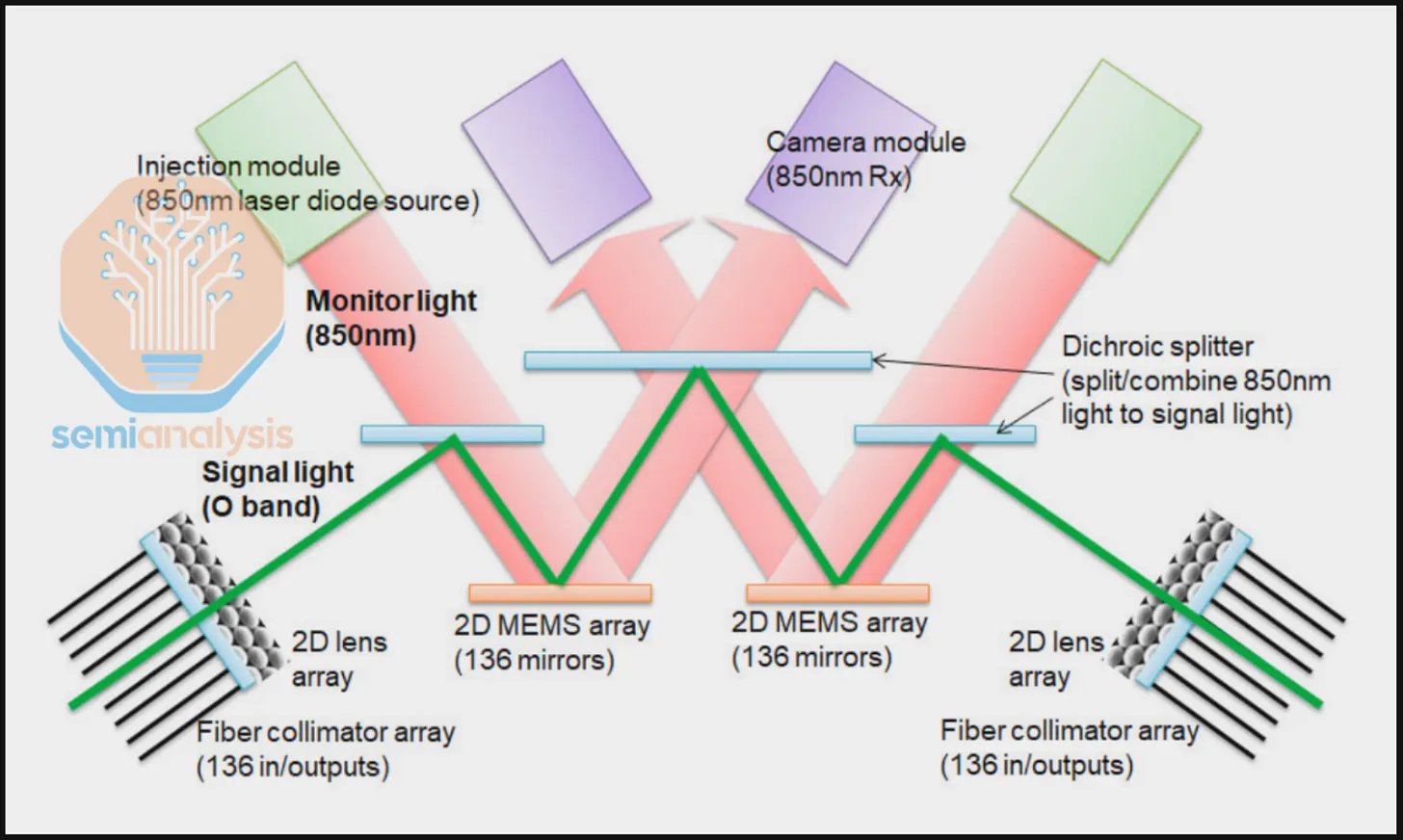
The Performance Leap: It eliminates network contention. In a 16,000-chip pod, 3D-optimized topology, no chip ever waits to talk to another. Latency and bandwidth become predictable, not probabilistic.
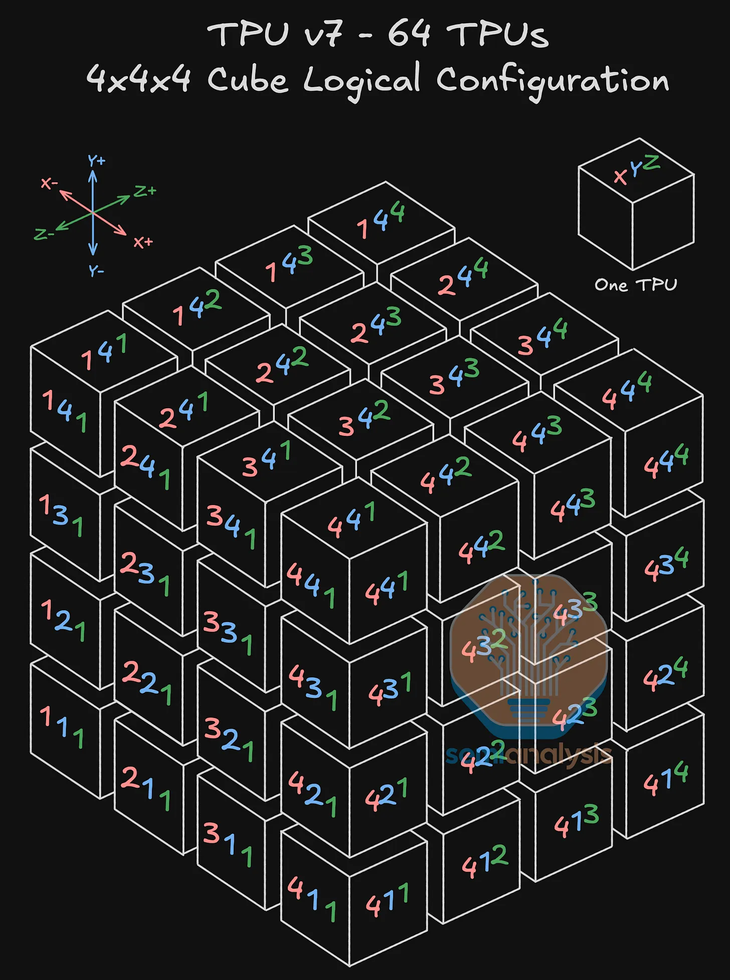
The problem of arranging these TPUs optimally is a well-known problem in math called graph partitioning. An optimal solution – often requiring connecting exponential higher wires between TPUs – is the Clos network. However, this network topology is still too prohibitive for real-world applications. The optimal – constrained to minimizing wire connections or graph edges – is known as torus interconnect, and it is extremely efficient for parallelizable nodes like that of a massive TPU compute unit using extremely parallelizable transformer-based LLMs (mainly matrix multiplications).
The Efficiency Gain: Traditional networks are over-provisioned for peak load, leading to idle capacity. The OCS dynamically rewires the physical network to perfectly match the AI model’s communication pattern, driving utilization to near 100%. This is a structural cost advantage that no competitor using commodity Ethernet ($ANET) or InfiniBand ($NVDA) can match – this is a physical limitation of nature that Jensen Huang cannot overcome.
Why 2026 is the Inflection Point
The AI market is maturing. The initial phase was about capability at any cost. The next phase, beginning in 2026, will be about profitability at scale.
- Model Sizes Are Plateauing: The exponential growth in parameters is hitting physical and economic limits. The next gains will come from efficiency and scale of training, not just architectural novelty.
- The Agentic Shift: Agentic workloads require sustained, complex communication between models, not just single, massive training runs. The ecosystem with the most efficient internal “nervous system” will win.
- Capex Rationalization: Hyperscalers facing investor pressure on capital expenditure will be forced to adopt more efficient, ASIC-based infrastructures over costly, generalized GPU clusters.
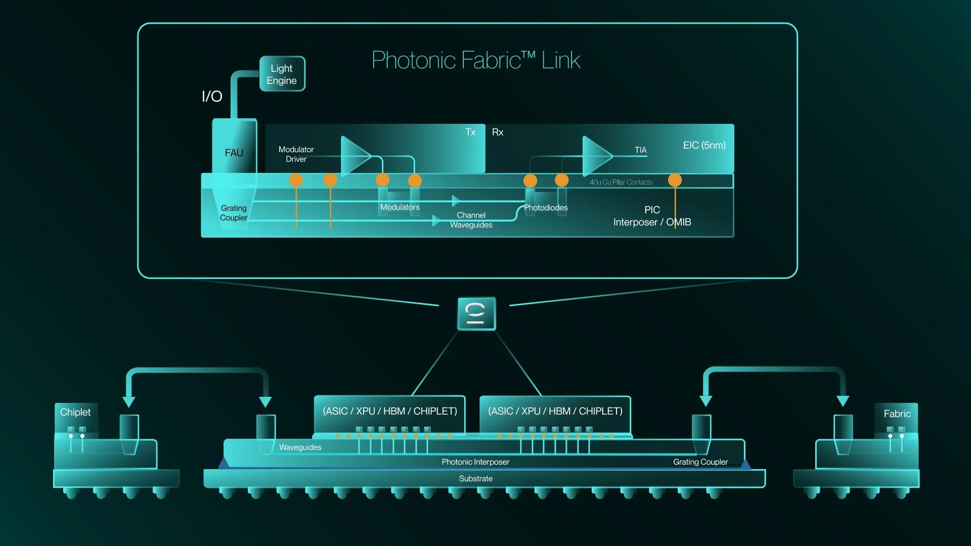
So what will the AI datacenters of the future look like? First, the datacenters themselves will be in a geographically power-constrained distributed network. Within each datacenters, to maximize computer/datacenter, locally distributed ASICs like TPUs will be connected by an optical network leveraging optical transceivers and OCS.
Investment Implications
The emergence of optical distributed network computing creates a clear bifurcation in AI infrastructure, making the Google Complex a more compelling structural bet over the OpenAI complex for the 2026 AI infra buildout.
Base investment case:
- Overweight Google $GOOGL: They are the only player with a deployed, scaled OCS network (TPU v7). This is a 3-5 year architectural lead that turns AI demand directly into margin.
- Overweight Broadcom $AVGO: The primary beneficiary of the “ASIC-ification” of the cloud. As other hyperscalers race to build their own custom silicon to compete with Google’s efficiency, Broadcom is the indispensable design and manufacturing partner.
- Tactical Nvidia $NVDA: Remains a toll-road on the OpenAI complex, but use options (debit call spreads make sense) for capital-efficient convexity. However, its growth story faces headwinds as the market rewards efficiency over raw, expensive FLOPS.
High-conviction bet:
- Lean into the real photonics tech like $LITE and $COHR, not merely those who are “AI-adjacent” like $POET. Photonics is a highly technical (even for electrical engineers) so don’t trust PR or non-technical investors assessment of near-term commercial viability.
- The investment opportunity for MEMS (Silex $SILXF, STMicroeletronics $STM) in OCS belongs exclusively to the specialized foundries capable of manufacturing ultra-reliable, large-scale mirror arrays at precision tolerances for hyperscale customers, not the broader MEMS market focused on high-volume consumer sensors.

Leave a comment